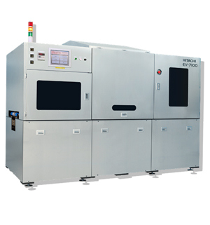
HIgh-tact time (the best level in the industry) as ever and applicable for larger size panel imaging with improvement of the transfer system. Mechanical cramp adopted to warp or high tack panel in solder resit process.
-
Imaging
Contact Exposure
-
L/S
75 /75 um
- PC/Motherboard
- HDI
- BGA
- CSP
- FC-BGA
- Package
- Specifications
Imaging Size 300×300
(Transmitted illumination: 300x535mm、 Thin plate: 330×635mm)Panel Thickness 0.1~3.2mm
(~2.4mm, Mechanical Cramp)Light Source [CL] Short-arc Lamp 5.0kW
[LR] Metal halide Lamp 12.0kW